Podcast Episode
The claim is striking because a 1.4-nanometre equivalent is expected to sit near the global frontier of advanced chipmaking around the end of the decade. If Huawei can reach it without the cutting-edge lithography machines that remain off-limits under US export controls, it would reshape assumptions about what is achievable under sanctions.
Built on this idea is a technology called LogicFolding architecture, which Huawei says reduces the resistive and capacitive load on signal propagation to boost transistor density. The company claims it has already used the new scaling law to design and mass-produce 381 chips over the past six years, and that new Kirin chips due to launch later this year will be the first to adopt the LogicFolding architecture.
Huawei Claims New Chip Architecture Can Match 1.4 nm by 2031
May 25, 2026
0:00
5:15
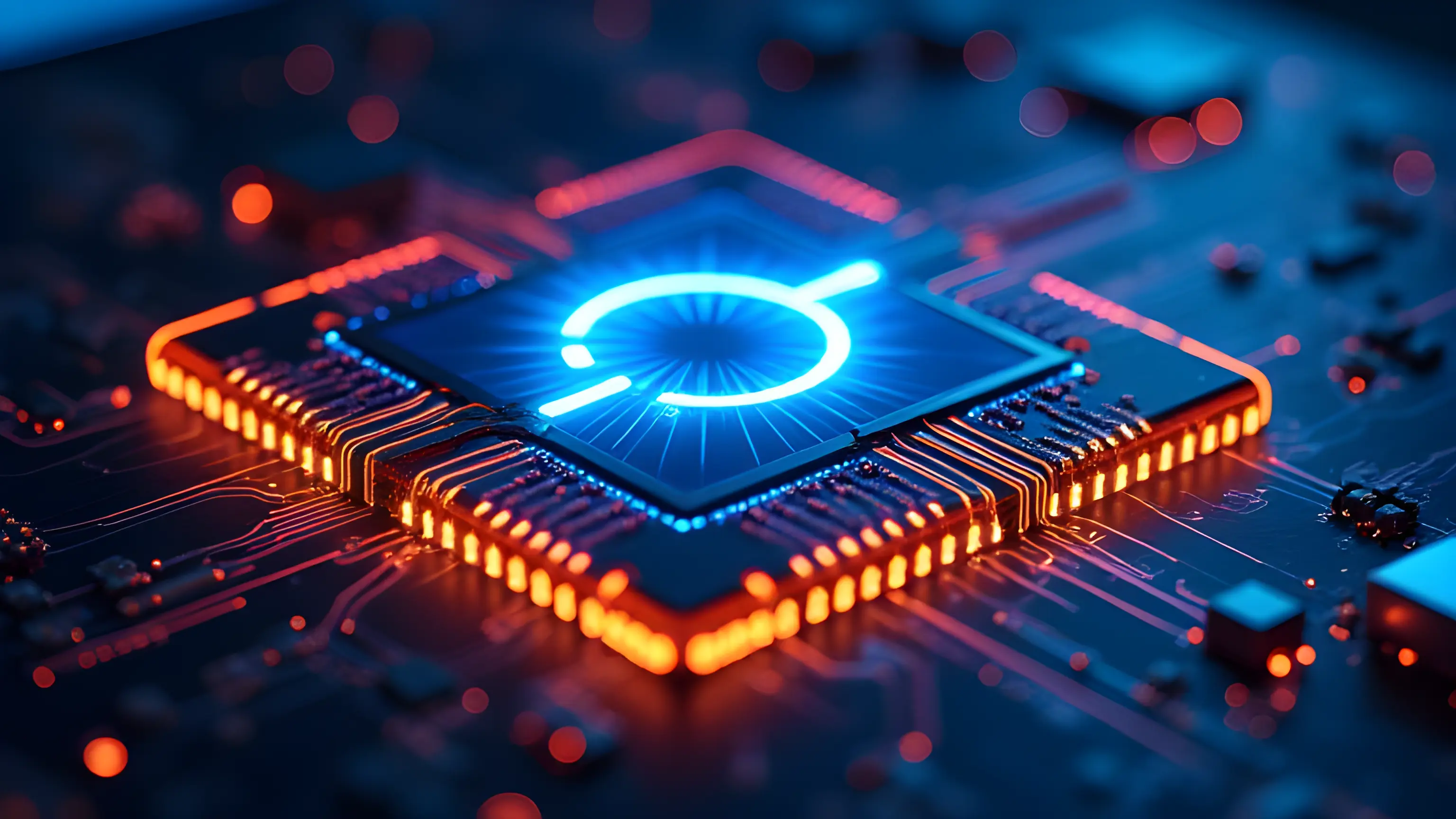
Huawei has unveiled a new chip design philosophy it calls the Tau Scaling Law, alongside a technology named LogicFolding, claiming it can deliver performance equivalent to a 1.4-nanometre process by 2031. The move is a bid to keep advancing despite US sanctions blocking access to the most advanced manufacturing tools.
A Bold Claim From Shanghai
Huawei Technologies has announced a new chip architecture and an accompanying design principle that it claims could bring its semiconductors to performance levels equivalent to a 1.4-nanometre process node by 2031. The announcement was made by He Tingbo, chair of Huawei's Scientist Committee and president of the company's semiconductor business department, during a keynote at the 2026 IEEE International Symposium on Circuits and Systems in Shanghai.The claim is striking because a 1.4-nanometre equivalent is expected to sit near the global frontier of advanced chipmaking around the end of the decade. If Huawei can reach it without the cutting-edge lithography machines that remain off-limits under US export controls, it would reshape assumptions about what is achievable under sanctions.
Rethinking How Chips Improve
The centrepiece is a principle Huawei calls the Tau Scaling Law, informally dubbed "Her's Law" by He's peers. Rather than relying solely on shrinking transistors ever smaller — the geometric miniaturisation that has driven the industry for decades — the approach emphasises what the company calls "time scaling," measuring and pursuing performance gains in a different way.Built on this idea is a technology called LogicFolding architecture, which Huawei says reduces the resistive and capacitive load on signal propagation to boost transistor density. The company claims it has already used the new scaling law to design and mass-produce 381 chips over the past six years, and that new Kirin chips due to launch later this year will be the first to adopt the LogicFolding architecture.
The Sanctions Backdrop
The announcement lands against a backdrop of sustained US restrictions. Since 2019, Huawei has been cut off from advanced chipmaking tools and leading-edge foundry services from firms such as ASML and TSMC. Its current chips, including the Kirin 9030 used in the Mate 80 smartphones, are manufactured by SMIC on a process analysts place somewhere between 7nm and 5nm — still trailing the industry's leaders. Reports from mid-2025 also indicated work with SMIC on a carbon-based 3nm design.An Open Question
Huawei did not provide independent performance data to back the 1.4-nanometre equivalent claim. Whether LogicFolding can genuinely deliver sub-2nm-class performance without extreme ultraviolet lithography — which China still cannot access — remains unproven. It is a question the global semiconductor industry will be watching very closely, because the answer touches not just one company's roadmap but the entire economics of who can build the world's most advanced chips, and how.Published May 25, 2026 at 12:21pm